Dead End: IBM Millipede
Abstract
Millipede was IBM’s attempt to store data the way a record stores music, mechanically, but at the scale of molecules. At IBM’s Zurich Research Laboratory, Peter Vettiger and the Nobel laureate Gerd Binnig built chips carrying 1,024 microscopic cantilevers, each with a heated tip that pressed pits about 10 nanometres wide into a thin polymer film and felt for them again to read. In June 2002 IBM announced a density of a trillion bits per square inch, about twenty times the best magnetic disks of the day, and the project aimed at a product the size of a postage stamp for cameras and phones by around 2007. Flash memory, falling in price every year, got to that market first and kept it, and hard disks overtook Millipede’s density on their own. No probe-storage product ever shipped. The heated tips found a second life as a tool for nanoscale lithography.
From Microscope to Memory
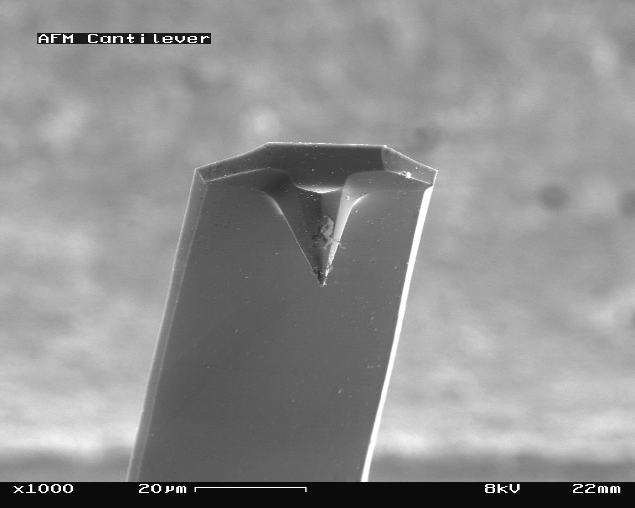
IBM’s Zurich laboratory in Rüschlikon had given the world a new way of seeing. In the early 1980s Gerd Binnig and Heinrich Rohrer built the scanning tunnelling microscope, which imaged individual atoms by scanning a sharp tip across a surface, and received half of the 1986 Nobel Prize in Physics for it (the other half went to Ernst Ruska for the electron microscope). In 1985 Binnig conceived a related instrument, the atomic force microscope (AFM), in which a tip on the end of a tiny flexible beam, the cantilever, touched the surface and the beam’s bending was measured. The AFM worked on any surface, not only conducting ones, and with Calvin Quate of Stanford and Christoph Gerber it became one of the standard tools of nanotechnology.
A tip that can feel a surface atom by atom can also change it. At IBM’s Almaden Research Center in California, John Mamin and Dan Rugar showed in 1992 that a heated AFM tip could write: they heated tips with microsecond laser pulses and pressed indentations about 150 nanometres wide into a polymer, and read them back with the same tip on a spinning disk. The obstacle to a memory was speed. One tip writing one pit at a time was hopelessly slow compared with a disk head. Binnig’s answer was parallelism: “Why not have thousands of cantilevers working in parallel?”
The Project
Peter Vettiger, an engineer at Zurich, and Binnig started the work in 1995, and IBM established it as an official project in 1996. They called it Millipede after the thousand legs. The team had to make an array of cantilevers in which every tip could be heated, addressed, and read individually, all on one silicon chip. They replaced the laser with resistive heaters built into each cantilever, added a Schottky diode to each so that one could be selected among many by row and column wires, and replaced piezoresistive sensors with a thermal reading method. In May 1998 an array of 1,024 cantilevers could read and write.
The working principle, as the project described it in 2002:
- Writing. A 32-by-32 array of 1,024 cantilevers, each about 70 micrometres long with a tip 2 micrometres high, sat over a thin film of polymer (PMMA, the material of Plexiglas) on a silicon substrate. To write a 1, a tip’s heater was raised to about 400 °C; the tip softened the polymer beneath it and sank in, leaving a pit as small as 10 nanometres.
- Reading. The heater ran at a lower temperature, about 300 °C, too cool to soften the polymer. Where a tip dropped into a pit, it came closer to the substrate and lost heat faster, and the heater’s resistance changed measurably.
- Erasing. Writing a new pit just beside an old one pushed up a rim that filled the old pit in.
- Moving. The tips did not move across the medium; the medium moved under the tips. Electromagnetic actuators shifted the polymer sled by up to 92 micrometres in each direction, so that each tip wrote and read only its own small field, all 1,024 in parallel.
The tips had to be uniform: their heights across the chip had to agree within 500 nanometres, and the team measured a standard deviation of 80 nanometres along one row. They proved robust: tips rewrote the same area more than 100,000 times without wearing out.
A Terabit per Square Inch
On 11 June 2002 IBM announced that the Zurich team had stored data at a density of a trillion bits (one terabit) per square inch, about twenty times the density of the best magnetic storage then available. The terabit figure came from a single tip writing pits about 10 nanometres apart; the full 1,024-tip array had read and written at 100 to 200 gigabits per square inch. Magnetic recording was then at 30 to 50 gigabits per square inch and aiming for a terabit in the future. “Because a nanometer-scale tip can address individual atoms, we anticipate further improvements far beyond this terabit milestone,” Binnig said. The next prototype was to have 4,096 tips in an array about 7 millimetres square.
The target market was mobile devices. A Millipede chip would be small, use little power when idle and be cheap to make, which suited digital cameras, music players, and phones, then storing their data on flash memory cards. Vettiger pointed out that it would hold more than flash memory of the same size. Calvin Quate called Millipede a “magnificent engineering achievement.” Thomas Albrecht of IBM’s own disk business was cooler: “I’m not sanguine about the prospects of any technology to replace magnetic recording in the next several years.”
The Race
IBM was not alone. By 2005 IEEE Spectrum counted a field of probe-storage efforts. Nanochip, a California start-up founded by Tom Rust and incorporated in 1996, wrote bits with probes in a phase-change material bought from Ovonyx, showed about a terabit per square inch in a 2004 prototype, and raised more than $20 million in February 2004 from investors including Microsoft; its chief executive expected a product within two years. Seagate ran a probe programme based on work at Carnegie Mellon University, and Samsung, Hitachi, Philips, and Hewlett-Packard had explored the idea, HP abandoning its programme. Developers expected the first probe drives on the market as early as January 2007.
In November 2004 the Zurich team stored and retrieved a text message at 517 gigabits per square inch, and in 2005 IBM showed a prototype with a 64-by-64 array at the CeBIT trade fair in Hanover. The tone of the project was cautious. “This is a research group, not a development laboratory,” co-manager Evangelos Eleftheriou told IEEE Spectrum; IBM had not decided whether to commercialise Millipede and was looking for a partner.
What Happened Instead
Flash memory took the market Millipede was built for. The flash business was worth about $4.8 billion in 2004, and Gartner expected $8.4 billion by 2008; every camera, phone, and music player was already designed around it, and its price per bit fell year after year as manufacturers shrank their cells (see Fujio Masuoka and Flash Memory). It had no moving parts at all, while Millipede still needed a mechanical scanner, however small. At the top end, hard disks kept improving: laptop drives reached 636 gigabits per square inch by late 2011, close to what Millipede had shown in the laboratory, without anyone having to build a new kind of device.
IBM never announced a product, and it never formally announced an end. From 2007 Eleftheriou’s group increasingly turned to other applications of its work. Nanochip did not ship a product either, and no company has sold a probe-storage device.
The Second Life
The heated tip outlived the memory. Zurich researchers developed new polymers, among them polyphthalaldehyde, a material first made at IBM in the 1980s, which a hot tip did not melt but broke into volatile fragments, so that material could be carved away layer by layer. In April 2010 IBM showed a three-dimensional relief map of the Earth in polyphthalaldehyde, 22 by 11 micrometres in size, so small that a thousand copies would fit on a grain of salt, written in 2 minutes and 23 seconds, and a model of the Matterhorn carved in 120 layers of a molecular glass whose bonds broke above 330 °C. The method made features as small as 15 nanometres. The technique, thermal scanning probe lithography, became a tool for making nanostructures in research laboratories; the Swiss company SwissLitho, founded in 2012 by two former IBM researchers and part of Heidelberg Instruments since 2021, sells instruments for it under the name NanoFrazor.
Dead End
Millipede was a research success and a product failure, and the reasons were economic, not physical. Its density was real, but density was not what customers of small storage devices were buying. They wanted a cheap, robust, solid-state component that already fitted every design, and flash was that component, improving on a predictable curve backed by the whole semiconductor industry. A new storage technology needs to be better than the incumbent’s next generation, not its current one, by the time it reaches the market, and Millipede’s target moved faster than it did.
Its own owner was also hesitant. IBM was leaving the hard-disk business while Millipede was in development (it sold its disk-drive division to Hitachi in 2002–2003), and a storage device that needed a manufacturing partner, a new supply chain, and a new interface had no obvious home inside it. The same fate met the start-ups in the field. The lesson is one that bubble memory and holographic storage had already taught: a storage medium competes not only with the technology it is meant to replace, but with that technology’s improvement rate.
📚 Sources
- Goldstein, Harry: “The Race to the Bottom,” IEEE Spectrum, 1 March 2005 (Binnig’s 1985 AFM and parallel-cantilever idea, Vettiger, Millipede established 1996, May 1998 1,024-cantilever array, November 2004 demonstration at 517 Gb/in², Eleftheriou quote, Nanochip, Seagate, Samsung, HP, flash market figures, 2007 market expectation)
- Levi, Barbara Goss: “Do Atomic Force Microscope Arrays Have the Write Stuff?,” Physics Today, 1 October 2002, doi:10.1063/1.1522154 (array geometry, write, read, and erase, actuators, uniformity, 100,000 rewrites, 100–200 Gb/in² versus 1 Tb/in², Quate and Albrecht quotes)
- “IBM Demonstrates Trillion-Bit Data Storage Density,” Enterprise Storage Forum, June 2002 (announcement of 11 June 2002, twenty times magnetic density, Vettiger and Binnig, 4,096-tip prototype)
- Eleftheriou, E. et al.: “Millipede: a MEMS-based scanning-probe data-storage system,” IEEE Transactions on Magnetics 39(2), 938, 2003
- Millipede memory, Wikipedia (PMMA medium, read heating to about 300 °C, CeBIT 2005 prototype, commercialisation target around 2007, flash and hard-disk density comparisons)
- Evangelos S. Eleftheriou, Wikipedia (team’s turn to other applications from 2007)
- Thermal scanning probe lithography, Wikipedia (Mamin and Rugar 1992, Millipede started 1995 by Vettiger and Binnig)
- “IBM Creates World’s Smallest 3D Map,” Nanowerk, 23 April 2010 (map 22 × 11 µm, 2 min 23 s, polyphthalaldehyde, Matterhorn in 120 layers, 15 nm features, Science)
- “IBM Research creates world’s smallest 3D map,” ScienceDaily, 24 April 2010 (polyphthalaldehyde map, Matterhorn in molecular glass, 330 °C, 120 layers, 15 nm)
- “Heidelberg Instruments celebrates 10th anniversary of NanoFrazor,” SEMI (SwissLitho founded 2012 by Felix Holzner and Philip Paul, part of Heidelberg Instruments)
- The Nobel Prize in Physics 1986 (Ruska; Binnig and Rohrer for the scanning tunnelling microscope)
- Image: AFM (used) cantilever in Scanning Electron Microscope, magnification 1000x.GIF by SecretDisc (CC BY-SA 3.0), via Wikimedia Commons