Fujio Masuoka and Flash Memory
Abstract
Fujio Masuoka (born 1943), an engineer at Toshiba, invented flash memory: a floating-gate memory that keeps its data without power and is erased electrically, a whole block at once, “like a camera flash.” He filed the first patent in 1980, presented the NOR version at the International Electron Devices Meeting in December 1984 and the denser NAND version in December 1987. He developed NAND largely without his employer’s permission, with two colleagues helping “under the desk,” because he wanted a semiconductor memory cheap enough to replace the hard disk. Intel brought the first commercial flash chip to market in 1988, Toshiba paid Masuoka a bonus that Forbes put at a few hundred dollars, and in 1994 he left for a university chair after Toshiba offered him a room without a team. NAND flash now stores the data in every phone, memory card and solid-state drive. In 2006 Toshiba settled his lawsuit over the invention for ¥87 million.
Takasaki and Sendai
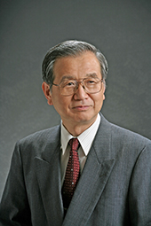
Fujio Masuoka was born on 8 May 1943 in Takasaki, Gunma Prefecture, north-west of Tokyo, into a small family of parents and two sisters. He went to school in Takasaki through high school and belonged to the physics and electronics club there; in high school he learned that the integrated circuit had been invented in the United States, and it became the first technology that interested him (see Jack Kilby and the Integrated Circuit). He told the Computer History Museum that he found technology easy to understand through mathematics, and that he had completed some university mathematics courses while still in high school.
He studied electrical engineering at Tohoku University in Sendai, graduating in 1966, and stayed for a doctorate on integrated circuits, which he completed in 1971. The same year he joined Tokyo Shibaura Electric, the company now called Toshiba.
Toshiba
His first assignment at Toshiba’s research centre was a floating-gate memory, and he worked on it alone under a single supervisor. In 1971 Intel had introduced the EPROM, a chip that stored bits as electric charge on a floating gate, an isolated piece of silicon surrounded by oxide, where the charge stayed for years without power. Erasing an Intel EPROM meant taking it out of its circuit and exposing it to ultraviolet light through a quartz window for 20 to 30 minutes. Masuoka’s version added a second gate, a control gate above the floating one, and could be programmed in about 100 microseconds. He presented it at the International Solid-State Circuits Conference in 1973; travel to an American conference was so expensive from Japan, he recalled, that a researcher went only if a paper had been accepted.
Toshiba then moved him to sales engineering for about two years, selling memory chips to American manufacturers although, by his own account, he could barely speak English. After that he went to the engineering division and worked on DRAM, where Toshiba was among the world leaders, including its one-megabit DRAM. Masuoka believed that the future lay in non-volatile memory instead. Microprocessors were spreading quickly, and every system that used one needed somewhere to keep its programs. Ultraviolet erasure made the EPROM awkward to use in a system; the electrically erasable EEPROM, which Intel put into practice as FLOTOX in 1980, needed a selection transistor for each cell so that every byte could be erased separately, which made each bit two transistors and limited how densely the chip could be packed.
Flash
Masuoka’s idea was to give up byte-by-byte erasure. If the selection transistor was removed and a whole block of cells was erased together, each cell could be a single transistor, and the memory could be made almost as dense as an EPROM while remaining electrically erasable inside the circuit. He filed the first patent, with his colleague Hisakazu Iizuka, in 1980. Another colleague, Shoji Ariizumi, said that erasing all the data at once reminded him of a camera’s flash, and the memory got its name.
In December 1984 Masuoka and four co-authors, M. Asano, H. Iwahashi, T. Komuro and S. Tanaka, presented “A new flash E²PROM cell using triple polysilicon technology” at the IEEE International Electron Devices Meeting (IEDM) in San Francisco. The cell used three layers of polycrystalline silicon for the floating gate, the control gate and a separate erase gate; it was written by tunnelling electrons onto the floating gate and erased in one operation by the erase gate. The cells were connected in parallel between a bit line and ground, the arrangement that gave this type its later name, NOR flash, after the logic gate whose transistors are connected the same way. Each bit needed less than a quarter of the area of existing EEPROM cells. In February 1985 the same team described a 256-kilobit flash chip at the International Solid-State Circuits Conference.
Toshiba did not push the invention, and Intel did. Intel brought the first commercial NOR flash chip to market in 1988, and NOR flash, with its fast random access, replaced ROM and EPROM as the program store of microprocessors and microcontrollers. Every major Japanese chipmaker came to sell single-chip microcontrollers with NOR flash on board for about a dollar each, Masuoka recalled, and they ran engine controls, consumer electronics and, later, the first mobile phones (see Andy Grove and Intel).
NAND
NOR flash was fast but could not be made cheap enough for what Masuoka had in mind. “The biggest memory market was the hard disc area,” he said in 2012, and he wanted a semiconductor memory that could compete with the disk (see The Storage Revolution).
The opportunity came from a lawsuit. In 1986 Texas Instruments brought a DRAM complaint against Toshiba before the US International Trade Commission, and Toshiba sent Masuoka to Washington to support its defence. After the first three months of hearings, his part of the case was mostly done, and in Washington he wrote about five patents on a new cell arrangement. In NAND flash the cells are connected in series, like the transistors of a NAND gate, in strings that share a single contact to the bit line. Removing most of the contacts made each cell much smaller than a NOR cell, at the cost of random access: data had to be read and written in pages, as on a disk.
Back in Japan, Masuoka started work on NAND “without permission,” as he put it; his official assignment at the time, he said, was nothing at all. Two colleagues helped him in their spare time, an arrangement he described with the Japanese expression “under the desk,” and the first test design took four weeks. He presented “New ultra high density EPROM and flash EEPROM with NAND structure cell” with Momodomi, Iwata and Shirota at the IEDM in December 1987.
When he asked for money to develop a four-megabit NAND chip, his boss told him there was none. Masuoka went instead to Hiseo Tajiri, the head of Toshiba’s consumer electronics development, and proposed that NAND flash could replace film in cameras. Tajiri was sceptical at first, then agreed, and the consumer division paid ¥100,000 for the work. In 1990 Tajiri’s group completed a digital camera that stored its pictures on eight four-megabit NAND chips, 32 megabits in all, with a CCD image sensor. It cost about $20,000 and nobody bought it. The camera engineers then left Toshiba together for Fuji Film, whose management had concluded that flash would one day replace film.
SmartMedia and Samsung
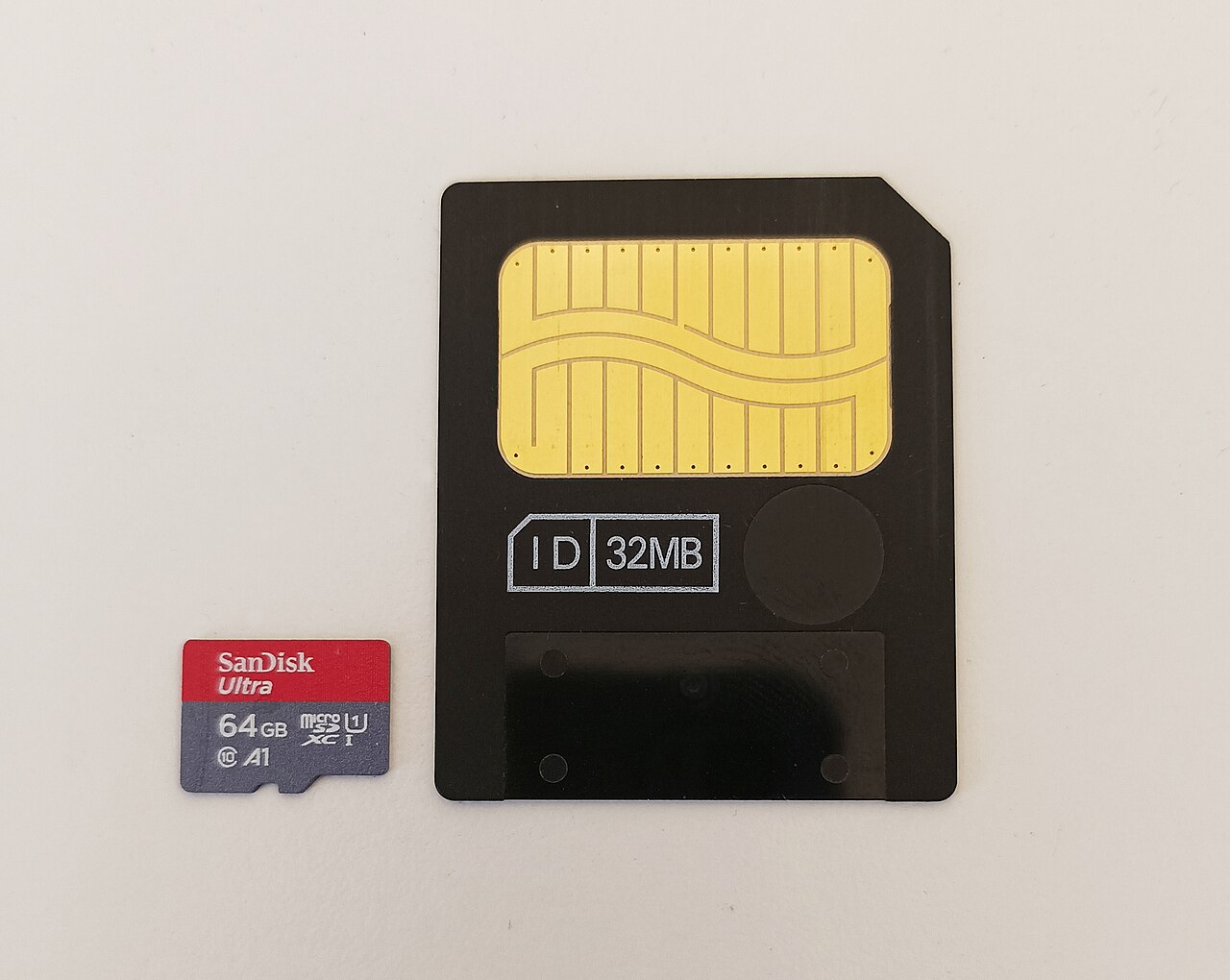
Turning NAND into a product took about four years, Masuoka said, with a team that never had more than ten people. The main problem was charge leaking off the floating gate: a DRAM cell has to hold its charge for a few milliseconds until the next refresh, while a flash cell must hold it for ten years, also at 100 °C. The solutions lay in the oxide quality, in cleaning the wafers and in the annealing conditions during production. The first chips survived about a thousand write-erase cycles, and process improvements raised that figure.
What finally changed Toshiba’s mind was Samsung. After Toshiba succeeded with the four-megabit chip, Samsung proposed developing a 16-megabit NAND chip together, and about 30 Samsung engineers came to Toshiba. Volume production of 16-megabit NAND began at both companies around 1996. By then Toshiba had introduced SmartMedia in 1995, the first removable memory card based on NAND flash; digital cameras were its first large market, followed by music players, USB drives, mobile phones and solid-state drives. NAND overtook NOR as the best-selling type of flash in 2005, and by 2010 the combined flash market exceeded $26 billion a year. “NAND flash memory made much money for Toshiba,” Masuoka said; the team that had been fewer than ten people grew, he estimated, to about a thousand engineers.
Leaving Toshiba
By 1994 Toshiba was making NAND flash in small quantities. Masuoka was a senior researcher who, by his own description, habitually went in direction B when his boss ordered A. When he asked about his future, he was offered a position with no supporting team and no research budget: “only one position,” he recalled, and “one room.” He left for Tohoku University, which made him a professor in its Graduate School of Information Sciences in 1994 and moved him to its Research Institute of Electrical Communication in 1996. If he had stayed at Toshiba, he said in 2012, he would not have led the flash work; he would have been one researcher alone.
At Tohoku he continued work he had started at Toshiba, where in 1988 a team led by him had demonstrated the surrounding gate transistor (SGT), a vertical transistor whose gate wraps all the way around a silicon pillar, the first gate-all-around transistor. He spent eleven and a half years at the university, retired in 2007 as professor emeritus under the Japanese age rule, and from 2004 also served as chief technology officer of Unisantis Electronics, a small company developing SGT-based designs, renamed Semicon Consulting in 2012. In later years his research turned to three-dimensional flash memory in which charge is stored in cylindrical cells stacked in many layers.
The Credit
In June 2002 Benjamin Fulford told Masuoka’s story in Forbes under the headline “Unsung Hero.” Toshiba, the magazine reported, had given him a bonus worth a few hundred dollars for the invention and had repeatedly tried to move him out of his senior post; asked who invented flash memory, Toshiba’s press department told Forbes that it was Intel, while Intel said it was Toshiba. The IEEE had given Masuoka its Morris N. Liebmann Memorial Award for the invention in 1997.
In 2004 Masuoka sued Toshiba in the Tokyo District Court for ¥1 billion (about $9 million) as compensation for his employee inventions. In July 2006 the two sides settled for ¥87 million (about $758,000), stating that there were “no longer any outstanding issues or liabilities between them in respect of these employee’s inventions.”
Recognition in Japan followed. He received the Medal with Purple Ribbon in 2007, was named a Person of Cultural Merit in 2013, received the Order of the Sacred Treasure, Gold and Silver Star, and in 2018 the Honda Prize, with a citation for a memory that could erase 256 kilobits in a single batch and needed less than a quarter of the area per bit of earlier devices. In 2013 the Flash Memory Summit gave him its Lifetime Achievement Award. The Honda Foundation counted 189 patents, 79 papers and 114 conference presentations.
Asked in 2012 what he would tell young people who wanted to become scientists, Masuoka said that mathematics and physics were very important, and that they should study mathematics “from the basic step.”
📚 Sources
- Katz, Jeff: “Oral History of Fujio Masuoka,” Computer History Museum, recorded 21 September 2012, Mountain View, CHM Ref. X6623.2013 (transcript, 28 pages: Takasaki, Tohoku, the 1973 EPROM, NOR and NAND, the ITC case in Washington, “without permission,” “under the desk,” Tajiri and the 1990 camera, Fuji Film, Samsung, leaving Toshiba)
- Fujio Masuoka, Wikipedia (birth, degrees, patent with Iizuka, Ariizumi, SGT 1988, Tohoku, Unisantis, Forbes claims, honours)
- Masuoka, F., Asano, M., Iwahashi, H., Komuro, T. & Tanaka, S.: “A new flash E²PROM cell using triple polysilicon technology,” 1984 International Electron Devices Meeting, pp. 464–467
- Masuoka, F. et al.: “A 256K flash EEPROM using triple polysilicon technology,” 1985 IEEE International Solid-State Circuits Conference
- Masuoka, F., Momodomi, M., Iwata, Y. & Shirota, R.: “New ultra high density EPROM and flash EEPROM with NAND structure cell,” 1987 International Electron Devices Meeting
- “1984: Flash memory released (Toshiba),” Semiconductor History Museum of Japan (FAMOS, FLOTOX, the NOR cell, batch erase, the NAND structure, 2010 market figure)
- Flash memory, Wikipedia (Intel’s first commercial NOR chip in 1988, SmartMedia 1995, NAND overtakes NOR in 2005)
- “Honda Prize 2018 awarded to Dr. Fujio Masuoka,” Honda, 28 September 2018 (career dates, 256-kilobit batch erase, quarter of the area, patent and paper counts, Flash Memory Summit award, 3D flash research)
- Fulford, Benjamin: “Unsung Hero,” Forbes Global, 24 June 2002
- Ingram, Mathew: “He invented flash memory but he got nothing in return,” newsletter (summary of the 2002 Forbes article)
- “Toshiba settles with flash memory inventor,” The Register, 31 July 2006
- Image: 舛岡富士雄.jpg by 文部科学省大臣官房人事課栄典班 (Ministry of Education, Culture, Sports, Science and Technology of Japan) (CC BY 4.0), via Wikimedia Commons
- Image: SmartMedia 32MB SD card.jpg by RetroEditor (CC BY-SA 4.0), via Wikimedia Commons