Semiconductor Fabrication
Abstract
The transistor of 1947 was a laboratory curiosity; what made billions of them per chip possible was a sequence of process inventions, mostly at Bell Labs and Fairchild in the 1950s. Zone refining (1951) made germanium and silicon pure enough to control. Crystal growing and diffusion set the impurities where they were wanted. Oxide masking (1955), discovered when a furnace fire filled a tube with steam, and photolithography (1955) let engineers draw patterns on silicon and dope only the exposed parts. Jean Hoerni’s planar process (1959) and epitaxy (1960) turned these steps into a flat, repeatable recipe on which every integrated circuit since has been built. In 1974 Robert Dennard’s scaling rules explained why shrinking it all made chips faster and cheaper; around 2005 that stopped being true.
Purity
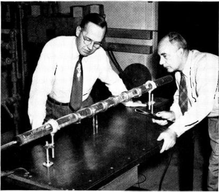
The first transistors were made from germanium contaminated well beyond what their designers could control (see The Transistor). In 1950–51 William Pfann at Bell Labs found a way to clean it. He passed a long tube of germanium slowly through a series of heating coils; each coil melted a narrow zone, and as the zone moved along and the metal refroze behind it, impurities stayed in the liquid and were swept to the end of the bar. Repeated passes brought impurities down to about one part in ten billion. Keck and Golay at the Army Signal Corps laboratory in Fort Monmouth and R. Emeis at Siemens in Pretzfeld developed the same idea independently. Silicon, which melts at a much higher temperature and reacts with any container, needed a variant: from 1952 Henry Theurer at Bell Labs clamped a silicon rod vertically and moved a single heating coil along it, so that surface tension held the molten zone in place without a crucible. By early 1955 his float-zone silicon was below one part per billion.
Pure material also had to be one crystal. Bell Labs chemist Gordon Teal, with John Little and Ernest Buehler, grew single crystals of germanium by dipping a seed crystal into the melt and slowly pulling it out, the method Jan Czochralski had described in 1917. From April 1950 Teal and Morgan Sparks dropped pellets of impurities into the melt during growth, producing a crystal with a thin p-type layer between two n-type layers. These grown-junction transistors, announced by Bell Labs at a press conference with William Shockley on 4 July 1951, outperformed the point-contact transistor (see William Shockley). Shockley later called Teal’s crystal growing “the most important scientific development in the semiconductor field in the early days”.
Diffusion
Growing junctions into a crystal gave little control over their thickness. In 1952 Calvin Fuller at Bell Labs showed that impurity atoms in a hot gas would diffuse into the surface of germanium or silicon, and that the time and temperature of exposure set how many entered and how deep they went, to better than a micrometre. Early in 1954 Fuller, Daryl Chapin and Gerald Pearson diffused boron into silicon to make the first practical solar cells, announced on 26 April 1954 with efficiencies up to 6 per cent. Later that year Charles Lee used diffusion to make transistors with base layers a micrometre thick, working at up to 170 MHz, ten times faster than before, and in March 1955 Morris Tanenbaum and D. E. Thomas made diffused-base silicon transistors.
Oxide and Light
Diffusing at high temperature pitted the surface of silicon wafers. Early in 1955 Carl Frosch and Lincoln Derick at Bell Labs found a cure by accident: hydrogen in their diffusion furnace caught fire, the water vapour it produced oxidised the wafers, and the layer of silicon dioxide sealed them. Over the following months they worked out which impurities the oxide blocked and how to etch openings in it, so that dopants entered the silicon only where the oxide had been removed. Their patent was filed on 2 December 1956 and issued on 13 August 1957; the paper appeared in September 1957. Germanium has no comparably stable oxide, and this is one of the reasons silicon replaced it.
Openings in the oxide had to be drawn. In 1955 Jules Andrus and Walter L. Bond at Bell Labs adapted photoengraving from the printing trade: a light-sensitive resist was exposed through a mask, developed, and used as a stencil for etching the oxide. In 1957 Jay Lathrop and James Nall of the Army’s Diamond Ordnance Fuze Laboratories patented a photolithographic process that deposited metal strips about 200 micrometres wide and etched holes in silicon dioxide for arrays of diodes. At Fairchild in 1958 Jay Last and Robert Noyce built one of the first step-and-repeat cameras, which repeated a single pattern many times across a wafer, so that one wafer yielded many identical transistors.
Planar and Epitaxial
Fairchild’s first transistors were mesas: diffused silicon whose junctions were exposed at the edges of etched plateaus, where dirt and moisture could reach them. Jean Hoerni proposed the opposite of standard practice: leave the oxide on after diffusion, so that it protected the junctions where they met the surface. He filed a patent disclosure in January 1959, had working devices in March, and Fairchild sold the first planar transistor, the 2N1613, from April 1960. All the structures of a planar device lay in one surface and were made from one side of the wafer, which allowed Noyce to connect several of them with a metal layer on top of the oxide: the planar integrated circuit (see The Integrated Circuit Revolution and Robert Noyce and Fairchild Semiconductor).
Epitaxy, growing a thin layer of crystal on a substrate so that it continues the underlying lattice, had been tried by Teal and Howard Christensen in 1951. In 1960, urged by Ian Ross, Theurer’s group at Bell Labs grew epitaxial silicon layers by chemical vapour deposition and used them to make transistors with higher breakdown voltage and faster switching; Theurer presented the results in June 1960. Fairchild’s epitaxial 2N914 followed in March 1961, and the process spread to Western Electric, Texas Instruments, Motorola and others within months.
Clean Rooms and Equipment
Smaller structures made dust a killer. In 1960 Willis Whitfield at Sandia National Laboratories designed the laminar-flow clean room, in which a constant stream of filtered air flushes particles out of the working space; it became the standard environment for chip making.
In the early years each company built its own furnaces and cameras; Jack Kilby recalled early equipment costing less than $10,000. From the 1960s outside suppliers took over: Electroglas, a Fairchild spin-off of 1961, made wafer probers, Kulicke & Soffa sold contact aligners from 1965, GCA’s David W. Mann division was the first commercial maker of step-and-repeat reduction cameras in 1961, and Applied Materials was founded in 1967 to sell chemical-vapour-deposition systems. Chip companies could then buy their process rather than invent it, which in the 1980s made room for foundries that built other firms’ designs and for fabless companies that only designed (see Morris Chang and TSMC). Wafers grew from half an inch across in 1958 to 300 millimetres.
In 1967 Robert Kerwin, Donald Klein and John Sarace at Bell Labs replaced the aluminium gate of the MOS transistor with polycrystalline silicon. At Fairchild in 1968 Federico Faggin and Tom Klein turned the silicon gate into a production process and made the first commercial silicon-gate chip, the 3708; it gave three to five times the speed in half the area, and Faggin took it to Intel, where it built the 4004 (see Federico Faggin and the Microprocessor).
Scaling
In 1974 Robert Dennard and five IBM colleagues published “Design of ion-implanted MOSFET’s with very small physical dimensions” in the IEEE Journal of Solid-State Circuits. They showed that if a MOS transistor’s dimensions and voltages were all reduced by the same factor, it switched faster by that factor while its power per unit area stayed constant. At the time IBM’s MOS memories used 5-micrometre features. The paper gave a physical basis for Gordon Moore’s observation that the number of components per chip doubled at a regular pace (see Gordon Moore and Moore’s Law), and set the target the industry followed for thirty years; by 2006 features were below 100 nanometres.
Around 2005–2007 Dennard scaling broke down. Leakage current and threshold voltage do not shrink with the transistor, so power density rose with every generation instead of staying flat. Clock frequencies stopped climbing, and manufacturers put several processor cores on one chip instead, accepting that not all of a chip can be switched on at once within its power budget. Lithography went on shrinking, at rising cost, until the extreme-ultraviolet machines of a single supplier, ASML, became necessary for the smallest features (see The Semiconductor Race).
📚 Sources
- Computer History Museum, The Silicon Engine: timeline
- Computer History Museum, The Silicon Engine: 1951, Development of Zone Refining
- Computer History Museum, The Silicon Engine: 1951, First Grown-Junction Transistors Fabricated
- Computer History Museum, The Silicon Engine: 1954, Diffusion Process Developed for Transistors
- Computer History Museum, The Silicon Engine: 1955, Development of Oxide Masking
- Computer History Museum, The Silicon Engine: 1955, Photolithography Techniques Are Used to Make Silicon Devices
- Computer History Museum, The Silicon Engine: 1959, Invention of the “Planar” Manufacturing Process
- Computer History Museum, The Silicon Engine: 1960, Epitaxial Deposition Process Enhances Transistor Performance
- Computer History Museum, The Silicon Engine: 1967, Turnkey Equipment Suppliers Change Industry Dynamics
- Computer History Museum, The Silicon Engine: 1968, Silicon Gate Technology Developed for ICs
- Computer History Museum, The Silicon Engine: 1974, Scaling of IC Process Design Rules Quantified
- Robert H. Dennard et al., “Design of ion-implanted MOSFET’s with very small physical dimensions”, IEEE Journal of Solid-State Circuits 9:5 (October 1974)
- Wikipedia: Dennard scaling
- Wikipedia: Willis Whitfield